Introduction
Von Neumann Architecture
The first computers had fixed programs and changing a computer program required physically rewiring or redesigning the machine. This meant that re-repurposing an computer was a difficult, expensive and time-consuming process.
The Mathematician John Von-Neuman designed the specification for the first programmable computer in 1954, where the programs themselves could be stored in memory, not just data.
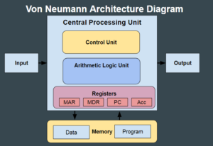
Instructions are stored in memory and are retrieved and processed by the Central Processing Unit one by one. This blueprint is known as the Von-Neumann Architecture.
The Von-Neuman Architecture is based on the principle of:
- Fetch an Instruction
- Decode the Instruction
- Execute the Instruction
The process above is repeated indefinitely, and is known as the fetch, decode, execute cycle.
Video
Tutorial Videos
Video 1
Video 2
The Google Slides blank document to follow along with the video is available here.
CU
Control Unit (CU) & System Clock
The job of the control unit is to coordinate and control all the other parts of the CPU. It tells the registers & ALU what to do with an instruction that is passed to them.
The CU decodes the instructions retrieved from memory and instructs the ALU to perform an arithmetic or logic instruction on the data from the decoded instruction.
ALU
Arithmetic Logic Unit
They job of the ALU is to perform the calculations or logic that the CU has decoded.
Common processes include:
- Addition
- Subtraction
- Division
- Multiplication
- Selection / Branching
- Repetition / looping.
Registers
Registers
The registers form part of the CPU Cache, temporarily storing data ready for processing or send to the RAM.
PC – Program Control Register
The program control register stores the address of the current instruction. Once the current instruction has been fetched and decoded, the program control register changes to the address of the next instruction.
IR – Instruction Register
The instruction register contains the current instruction itself, retrieved from it’s stored address.
MAR – Memory Address Register
The memory address register contains the memory location of either the next instruction to be fetched or the location of where the results of the current process are to be stored.
MDR – Memory Data Register
The memory data register contains either the data retrieved from memory (either an instruction or an operand) during the current fetch cycle at the address stipulated in the MAR, or the data the is due to be written to memory.
ACC – Accumulator
The accumulator receives the results of the current process from the ALU and stores it for the use in the next Fetch-Decode-Execute cycle.
IX – Index Register
This register is used when performing operations involving index addressing.
Buses
Buses
Buses are the physical wires along which data is passed, both within the CPU itself and across the motherboard.
CPU Bus
The CPU bus is used to pass data around the CPU between the CU,ALU and registers.
Control Bus
The Control bus sends signals to the RAM, indicating whether to initiate a read or write on the address received along the address bus
Address Bus
The address bus is the wire along which the address of the memory location in RAM required for the read/write is sent.
Data Bus
The data bus is the wire along which the data is sent either to or from the RAM (depending whether a read or write has been initiated.
Quiz
Activity
Activity
Make a copy of this Google Slides ( File > Make a copy ) and fill in the blanks from the video
Von Neuman Blank Copy